MIT has found a way to get electronics into hard-to-access places, by flowing it in as a colloid or blowing it in on a puff of air.
 |
Colloids, milk is one, are suspensions of particles in a liquid that never settle out. And almost the same can be done in a gas, with dust particles, for example, taking hours or days to settle.
To created a circuit so light that it will both remain suspended in water and float in air, the MIT team turned to ‘two-dimensional’ materials – the most famous of which is graphene.
“We wanted to figure out methods to graft complete, intact electronic circuits onto colloidal particles,” said MIT chemistry professor Michael Strano.
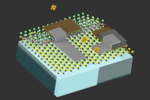
In this case, the colloidal particles are thin squares of epoxy 100μm across (four shown), on which the 2D materials and metal electrodes are deposited.
 |
“Particle buoyancy approaches the values of water droplets in
clouds. Sedimentation speed is ~20μm/s, allowing them to stay in the air for days,” according to ‘Colloidal nanoelectronic state machines based on 2D materials for aerosolizable electronics‘, a paper on the work in Nature Nanotechnology.
On the particle, connected in series, are: a photo-diode for power, a resistance-based chemical sensor and a memristor.
While the researchers describe the circuit as a state-machine, its operation can be summed up as: The memristor is made in a high-resistance state, and then adopts a permanent low-resistance state only if the particle is exposed to both light and the chemical it is designed to detect.
The 2D materials used were: graphene (a conductor), hexagonal boron nitride (hBN, an insulator), molybdenum disulphide (MoS2, a semiconductor) and tungsten diselenide (WSe2, a semiconductor). The two latter materials are in the form of transition-metal dichalcogenides.
Together, MoS2 and WSe2 can form a p-n hetero-junction for the photo-diode, connected through gold electrodes, the chemical sensor is a MoS2 between silver electrodes, and the memristor is a gold-MoS2-silver junction (its silver electrode is the table-tennis-bat-shaped thing in the above photo, over a grey MoS2 square).
A layer of hBN is used where insulation is needed, and as a passivation layer to keep the environment out of everything except the sensor.
Power from the photo-cell is “enough to let them sense information about their environment, store those data in their memory, and then later have the data read out after accomplishing their mission,” said MIT.
In figures, this is 30-100nW from the photo-cell, and the memristor needs only 30nW to irreversibly record events, changing its own conductivity up to 150x.
The active layers contribute almost no mass or thickness to the underlying epoxy flake. “With a thickness of 1.24μm and weight of ~1.4g/m2, this design represents
one of the thinnest and lightest circuits produced so far,” according to the paper.
Such tiny particles are almost impossible to find once released, so the researchers made them reflective by depositing silver over a 3D castellated structure on the surface. The resulting reflective right-angled mirrors allowed two-bounce corner-reflection, making the particles visible to a laser scanner when angled at up to 60° from the normal, and visible from the rear though the transparent flake body.
Work is under-way, said MIT, to add a timing mechanism to indicate when sensing activity occurred.
Such devices could ultimately be used for the oil and gas industry, said Strano, with particles flowed through pipelines to check for leaks or other issues.
Source from:electronicsweekly

 영어
영어  중국어
중국어  독일어
독일어  한국어
한국어  일본어
일본어  Farsi
Farsi  Portuguese
  Russian
  스페인어
스페인어 


